CXD-Q Amplifier GPIO Component

This topic describes how to configure and control the General Purpose Input Output (GPIO) hardware interface for the CXD-Q Amplifier in Q-SYS Designer.

The GPIO Controller is used to integrate Q-SYS with custom or third-party controls. Using the GPIO, Q-SYS can control external hardware and certain aspects of Q-SYS can be controlled by external hardware.

The GPIO Interface is physical hardware, and is represented in Q-SYS Designer by the GPIO component. There are eight configurable GPIO pins on the CXD-Q GPIO component. You can configure these pins to be Digital Inputs, Digital Outputs, Analog Inputs, or PWM Output. Refer to the Properties section in this topic for details.

Controls

The Controls are displayed in GPIO Pin number order, 1 through 8, from left to right in the Control Panel. For each control the Euro-style connector pin number is listed under the GPIO pin numbers. Refer to the GPIO Interface section in this topic.

Control

Function

Default / Range

Digital In

(Indicator)

This LED lights when there is a Digital input of 1 (3.3 V TTL) present.

Default = On

Range = On / Off

Analog In

Volts

This knob controls the analog input level up to 3.3 V

Default =

Range = 0 - 3.3

Digital Out

This toggle button supplies:

0 VDC output in the 0/Off position and

3.3 VDC output in the 1/On position.

Default = Off

Range = Off / On

PWM Duty

%

Sets the duty cycle of the pulse.

Default = 0

Range = 100

PWM Invert

Inverts the PWM pulse.

Default = +

Range = + / 1

PWM Frequency

Hz

Sets the frequency of the pulse. If there are multiple PWM assignments for one amplifier, all are controlled by the same frequency control.

Default = 50.0

Range = 5 to 50.0 k

Relay

This button changes position of the internal relay.

N / A

Properties

What you select in the Properties determines the use of that GPIO pin, unused, input, output, or clock.

Property

Function

Choices

Name

Identifies the CXD-Q component in Q-SYS Designer, enabling the connection between the design and the physical CXD-Q. This name should be the same as the CXD-Q Device Name (hostname Hostnames may contain ASCII letters 'a' through 'z' (case-insensitive), the digits '0' through '9', the hyphen, and the underscore. Hostname labels cannot begin or end with a hyphen. No other symbols, punctuation characters, or blank spaces are permitted. ) in the Q-SYS Configurator. Click the Name property and type the Name.

The name must follow standard naming conventions. The Administrator restricts the name according to the following:

ASCII characters a - z (case insensitive)

Digits 0 - 9

Hyphen (cannot be at the beginning or end of the name)

Underscore (acceptable with a Q-SYS implementation)

No other characters, symbols, punctuation, or blank spaces.

User input

Location

User defined Location for the CXD-Q

User input

GPIO 1 – GPIO 8

Configures the GPIO for the CXD-Q.

GPIO 1 - 8 have the options Unused, Digital Input, Analog Input, and Digital Output.

GPIO 1 through 4 and 6 add the PWM Output

.

Unused

Digital Input

Analog Input

Digital Output

PWM Output


GPIO Pin Selections

Value

Digital Input
(TTL 3.3 VDC @ 2 mA)

Digital zero = 0

Digital one = 3.3

Analog Input


Digital Output

0 or 1

PWM Output


Control Pins

The available Control Pins depend on settings in Properties. There is one control pin for each GPIO pin that has either Digital Input, Analog Input or Digital Output selected in the Properties. The GPIO Pins that have Unused will not have a Control Pin associated with it. For PWM there is a Duty and Invert for each PWM selected in the Properties, and one PWM Frequency for all of the PWM Outputs are selected in the Properties.

Pin Name

Value

String

Position

Pins Available

Digital Input

0

1

false

true

0

1

Output

Analog Input

0 to 3.3

0.00 V to 3.3 V

0 to 1.00

Output

Digital Output

0

1

false

true

0

1

Input / Output

PWM Duty

0 to 100

0 to 1.00

Input / Output

PWM Invert

0 to 100

0 to 1.00

Input / Output

PWM Frequency

5.00 to 1000

5.00 Hz to 50 kHz

0 to 1.00

Input / Output

Relay Out

0

1.00

false (normal)

true (activated)

0

1.00

Input / Output

GPIO Interface

Connector Pin

GPIO # and Function

Specification

16-pin Euro Style Connector
1

3.3 V

100 mA max (power cycle to reset current limiting IC)
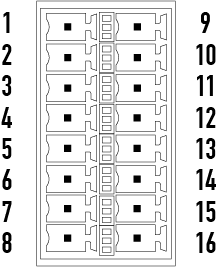
2

GPIO 1

5mA in/out, 3.3V max, 127 Ohm resistor in series

3

GPIO 2

5mA in/out, 3.3V max, 127 Ohm resistor in series

4

GND

Ground

5

GPIO 3

5mA in/out, 3.3V max, 127 Ohm resistor in series

6

GPIO 4

5mA in/out, 3.3V max, 127 Ohm resistor in series

7

GND

Ground

8

GPIO 5

18mA in/out max, 3.3V max, 127 Ohm resistor in series

9

RELAY NO

Relay Normally Open

10

RELAY COM

Relay Common

11

RELAY NC

Relay Normally Closed

12

GND

Ground

13

GPIO 6

18mA in/out max, 3.3V max, 127 Ohm resistor in series

14

GPIO 7

18mA in/out max, 3.3V max, 127 Ohm resistor in series

15

GND

Ground

16

GPIO 8

18mA in/out max, 3.3V max, 127 Ohm resistor in series

Examples

QSC.com | Software and Firmware | Resources | QSC Self Help Portal

© 2009 - 2018 QSC, LLC. All rights reserved. QSC and the QSC logo are trademarks of QSC, LLC in the U.S. Patent and Trademark office and other countries. All other trademarks are the property of their respective owners.

http://patents.qsc.com