What you select in the Properties determines the use of that GPIO pin, unused, input, output, or clock.
|
Property |
Function |
Choices |
|---|---|---|
|
Name |
Identifies the amplifier component in Q-SYS Designer, enabling the connection between the design and the physical device. This name should be the same as the amplifier Device Name (hostname Hostnames may contain ASCII letters 'a' through 'z' (case-insensitive), the digits '0' through '9', the hyphen, and the underscore. Hostname labels cannot begin or end with a hyphen. No other symbols, punctuation characters, or blank spaces are permitted. ) in the Q-SYS Configurator. The name must follow standard naming conventions, restricted to the following: ASCII characters a - z (case insensitive) Digits 0 - 9 Hyphen (cannot be at the beginning or end of the name) Underscore (acceptable with a Q-SYS implementation) No other characters, symbols, punctuation, or blank spaces. |
User input |
|
Location |
User defined Location for the amplifier. |
User input |
|
GPIO 1 – GPIO 8 |
Configures the GPIO for the amplifier. GPIO 1 - 8 have the options Unused, Digital Input, Analog Input, and Digital Output. GPIO 1 through 4 and 6 add the PWM Output . |
Unused Digital Input Analog Input Digital Output PWM Output |
|
GPIO Pin Selections |
Value |
|---|---|
|
Digital Input |
Digital zero = 0 Digital one = 3.3 |
|
Analog Input |
|
|
Digital Output |
0 or 1 |
|
PWM Output |
|
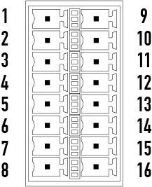
The Controls are displayed in GPIO Pin number order, 1 through 8, from left to right in the Control Panel. For each control the Euro-style connector pin number is listed under the GPIO pin numbers. Refer to the GPIO Interface section in this topic.
|
Control |
Function |
Default / Range |
|---|---|---|
|
Digital In (Indicator) |
This LED lights when there is a Digital input of 1 (3.3 V TTL) present. |
Default = On Range = On / Off |
|
Analog In Volts |
This knob controls the analog input level up to 3.3 V |
Default = Range = 0 - 3.3 |
|
Digital Out |
This toggle button supplies: 0 VDC output in the 0/Off position and 3.3 VDC output in the 1/On position. |
Default = Off Range = Off / On |
|
PWM Duty % |
Sets the duty cycle of the pulse. |
Default = 0 Range = 100 |
|
PWM Invert |
Inverts the PWM pulse. |
Default = + Range = + / 1 |
|
PWM Frequency Hz |
Sets the frequency of the pulse. If there are multiple PWM assignments for one amplifier, all are controlled by the same frequency control. |
Default = 50.0 Range = 5 to 50.0 k |
|
Relay |
This button changes position of the internal relay. |
N / A |
The available Control Pins depend on settings in Properties. There is one control pin for each GPIO pin that has either Digital Input, Analog Input or Digital Output selected in the Properties. The GPIO Pins that have Unused will not have a Control Pin associated with it. For PWM there is a Duty and Invert for each PWM selected in the Properties, and one PWM Frequency for all of the PWM Outputs are selected in the Properties.
|
Pin Name |
Value |
String |
Position |
Pins Available |
|---|---|---|---|---|
|
Digital Input |
0 1 |
false true |
0 1 |
Output |
|
Analog Input |
0 to 3.3 |
0.00 V to 3.3 V |
0 to 1.00 |
Output |
|
Digital Output |
0 1 |
false true |
0 1 |
Input / Output |
|
PWM Duty |
0 to 100 |
— |
0 to 1.00 |
Input / Output |
|
PWM Invert |
0 to 100 |
— |
0 to 1.00 |
Input / Output |
|
PWM Frequency |
5.00 to 1000 |
5.00 Hz to 50 kHz |
0 to 1.00 |
Input / Output |
|
Relay Out |
0 1.00 |
false (normal) true (activated) |
0 1.00 |
Input / Output |
|
Connector Pin |
GPIO # and Function |
Specification |
16-pin Euro Style Connector |
|---|---|---|---|
|
1 |
3.3 V |
100 mA max (power cycle to reset current limiting IC) |

|
|
2 |
GPIO 1 |
5mA in/out, 3.3V max, 127 Ohm resistor in series |
|
|
3 |
GPIO 2 |
5mA in/out, 3.3V max, 127 Ohm resistor in series |
|
|
4 |
GND |
Ground |
|
|
5 |
GPIO 3 |
5mA in/out, 3.3V max, 127 Ohm resistor in series |
|
|
6 |
GPIO 4 |
5mA in/out, 3.3V max, 127 Ohm resistor in series |
|
|
7 |
GND |
Ground |
|
|
8 |
GPIO 5 |
18mA in/out max, 3.3V max, 127 Ohm resistor in series |
|
|
9 |
RELAY NO |
Relay Normally Open |
|
|
10 |
RELAY COM |
Relay Common |
|
|
11 |
RELAY NC |
Relay Normally Closed |
|
|
12 |
GND |
Ground |
|
|
13 |
GPIO 6 |
18mA in/out max, 3.3V max, 127 Ohm resistor in series |
|
|
14 |
GPIO 7 |
18mA in/out max, 3.3V max, 127 Ohm resistor in series |
|
|
15 |
GND |
Ground |
|
|
16 |
GPIO 8 |
18mA in/out max, 3.3V max, 127 Ohm resistor in series |

