Connector Pin
GPIO # and Function
Specification
3.3 V
100 mA max (power cycle to reset current limiting IC)
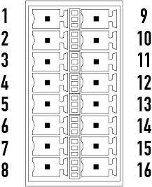
2
GPIO 1
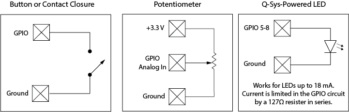
5mA in/out, 3.3V max, 127 Ohm resistor in series
3
GPIO 2
5mA in/out, 3.3V max, 127 Ohm resistor in series
4
GND
Ground
5
GPIO 3
5mA in/out, 3.3V max, 127 Ohm resistor in series
6
GPIO 4
5mA in/out, 3.3V max, 127 Ohm resistor in series
7
GND
Ground
8
GPIO 5
18mA in/out max, 3.3V max, 127 Ohm resistor in series
9
RELAY NO
Relay Normally Open
10
RELAY COM
Relay Common
11
RELAY NC
Relay Normally Closed
12
GND
Ground
13
GPIO 6
18mA in/out max, 3.3V max, 127 Ohm resistor in series
14
GPIO 7
18mA in/out max, 3.3V max, 127 Ohm resistor in series
15
GND
Ground
16
GPIO 8
18mA in/out max, 3.3V max, 127 Ohm resistor in series